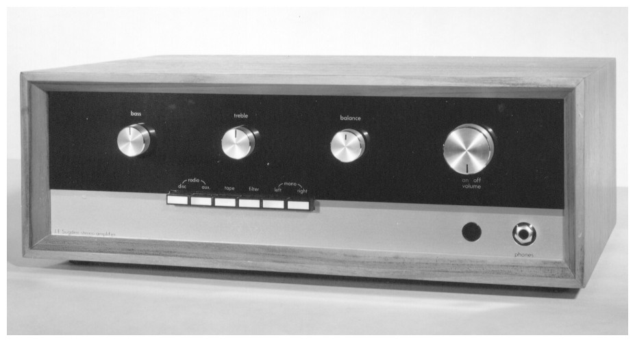
Although the Richard Allan version of the A21 made its debut in April 1968 it wasn’t long before it was replaced by a version with J. E. Sugden and Co on the front panel! The original Sugden A21 appeared before the end of 1968, and by mid-1969 around 500 had been sold.
If you compare the Richard Allan and JES A21’s they look very similar except for some styling changes that accompany the change in the displayed maker’s name and the addition of a headphone socket. The circuit design and specifications are also very similar.
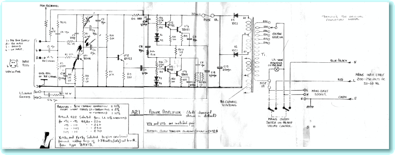
The above shows the original circuit diagram for the A21 as hand-drawn by Jim Sugden. If you wish to see a larger, more detailed version, click here. The specifications of the original JES A21 were the same as for the Richard Allan version, so I have not repeated them here. If you wish to see the specs then use the ‘back’ arrow at the bottom of this page to go to the page on the Richard Allan version.
The A21 proved very popular. As with other JES products it was not made on a production line basis. Instead each amplifier was assembled by an individual. This may have been slower than a production line, but it meant that each assembly worker could take pride in the specific items they had made.
Although the original A21 design worked well it was actually difficult to make in any quantity. The transistors available in the 1960’s were much poorer in performance than we can get in the 21st century. The main problems with the output transistors were:
- The performance varied significantly from one device to another.
- The performance was strongly temperature dependent.
- The maximum currents, voltages and powers they could reliably provide were modest.
- High temperatures reduced the safe current and power levels.
Even now, the Achilles Heels of simple Class A power amplifiers are the need to dissipate relatively large amounts of waste heat without anything overheating, and the relatively high quiescent current levels the devices have to endure. With simple fixed-bias designs the maximum available output power whilst maintaining Class A operation is also limited by the quiescent current level.
The A21 used a quiescent current level of around 0·9 Amps. This meant that the amplifier could only deliver output currents of double this in Class A operation. The rail voltage was around 30V, so the waste heat dissipated was almost 30W per channel. The initial A21 used BD121 NPN transistors as the output devices. The table below compares their basic characteristics with a modern example of a Silicon bipolar audio output transistor, the 2SC2922 NPN which has been used by to make some excellent audio power amplifier designs – e.g. for the AudioLab 8000 series.
| Device
|
Max Voltage
|
Max Current
|
Max Power
|
| BD121
|
35 V
|
5 A
|
45 W
|
| 2SC2922
|
180 V
|
17 A
|
200 W
|
The above may not look too bad at first glance. The BD121 was rated at 35V max, but the amp only used 32V. The current rating was 5A, but the peak Class A output was only 1·8, and the power per device (two per channel) was around 15W – well below the 45W maximum on the BD121 data sheet. Alas, as anyone who has designed with bipolar power transistors transistors will know, the problem is lurking in the small print! Note that 35V times 5A should equal 175 Watts. Yet the BD121 is only rated for 45 Watts max. This warns that we can’t have max voltage and max current at the same time and expect the device to survive Also, the 45 Watt rating assumes that the case of the transistor is at room temperature. However as it dissipates power its temperature will rise. To make things worse, early types of transistor like the BD121 had much poorer internal arrangements than a modern power transistor. This means that for a given power level, even if you can keep the case cool, the actual piece of silicon inside gets much hotter than a modern device. As the device heats up, two things occur. Firstly, the maximum ratings for reliable operation fall. So we can’t even get the above maximum values for more than a short time. Secondly, other properties of the device also alter with temperature.
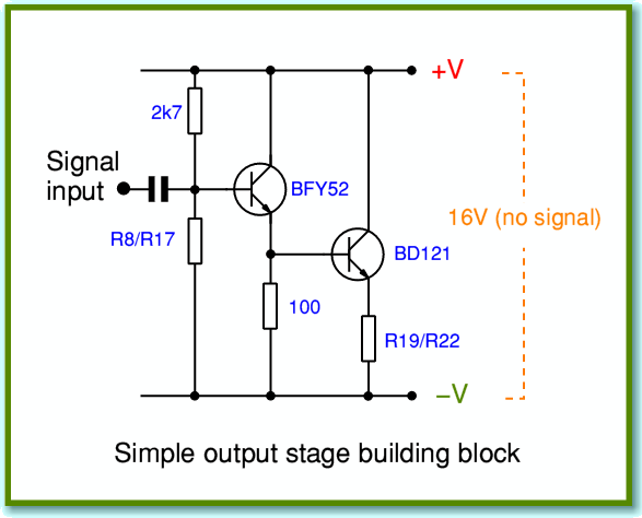
A simple push-pull output might have used two output stage ‘building blocks’ like the above. Here currents though the output devices are basically set by the choice of the resistor values. Provided that the resulting currents and powers are very low, the above design would be fine. However a real problem with early transistors was an effect known as “thermal runaway”. This is because the current through each transistor in a circuit like the above will tend to increase if we warm up the transistors. If we start with a high current, the transistors heat up to a high temperature. This causes the currents through them to also rise. The increase in current warms the transistors some more, which produces yet more current, which... The temperature and current rise steadily until something goes wrong or you switch off the circuit in alarm! The result may be anything from a fuse failure to the output devices blowing up as a result of overheating.
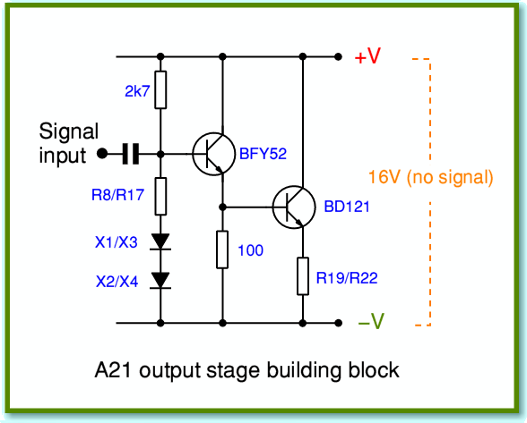
Jim Sugden initially tackled this in two ways. The first was to ensure the output devices had good heatsinks, minimising the temperature rise for a given power dissipation. The second was to employ a neat trick to stabilise the tendency of the current to change with temperature. The key part of the circuit is the use of the four carefully selected diodes shown on the early diagrams as X1 or X4. If you look at the circuit descriptions these were carefully chosen to have properties that matched the chosen pairs of output transistors.
The above shows how he modified the output building blocks by adding pairs of diodes (X1 and X2 in one block, X3 and X4 in the other) and carefully chose the resistor values to suit.
The trick was that these diodes warmed up whilst the amplifier was running, and tended to draw more current as things heated up. This reduced the input bias voltage applied to the first transistor of the building block. In effect it ‘bled away’ some of the current that would otherwise have been fed into the output devices, reduced the bias being fed to them. The result was that although the gain of the output devices was tending to increase, the input to them was being reduced by a corresponding amount. By choosing just the right combinations of diodes, transistors, and bias resistors, the gain was thermally stabilised and runaway avoided. The diodes also helped limit the maximum current you could demand from the output, protecting the fragile early transistors from being blown up by overenthusiastic use!
Unfortunately, although an ingenious solution, it meant that each amplifier had to be build using a very carefully matched set of components. As a result, in the early days one person was employed full-time just to measure and select the components for each individual amplifier. You can see some of the requirements specified on the circuit diagrams. This was quite a time-consuming process, but was vital for the original design to work well. It was one of the reasons that the original A21 was soon replaced by the redesigned ‘Series 2’ A21 before the end of 1969.